In my last tutorial, I talked about the TCA9548A MUX which can be used to add at the max of 64 I2C or I²C sensors to your Arduino/ESP8266/ESP32.
In this tutorial, I am going to talk about the PCF8574 8-bit GPIO Port Extender. It is one of the many GPIO extenders available in the market.
This tiny little board becomes a lifesaver When you run out of pins on your Arduino. This "GPIO (General Purpose Input Output) pin extender" provides an additional 8 pins (P0 ~ P7) which can be used to 'output a signal' or 'read a signal as an input'.
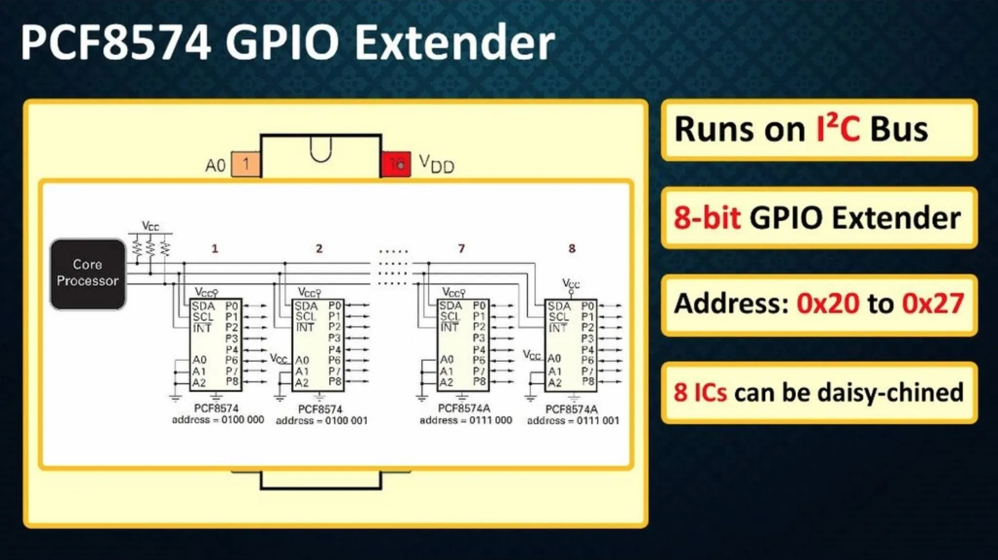
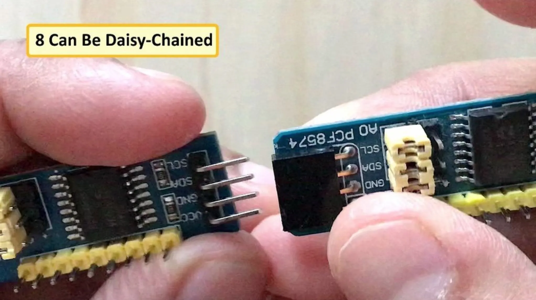
These modules run on the I2C bus, and if daisy-chained you can connect up to 8 of these devices in a project. Each device will give us an additional 8-bits of GPIO enabling 64 GPIOs in total.
These ICs are ridiculously cheap and can be bought easily from eBay or AliExpress. If you don't want to worry about the wiring and just want to keep your project really "simple", then you can buy these fully assembled breakout boards. You just need to hook them up to the I2C bus and you are all ready to go.
Step 1: Hardware Requirement
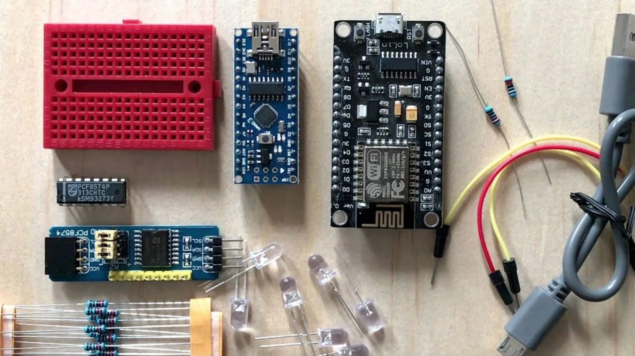
For this tutorial we need:
- Breadboard
- PCF8574 GPIO Extender IC
- PCF8574 GPIO Extender Breakout Board
- Arduino UNO/Nano whatever is handy
- NodeMCU
- Few LEDs and an equal amount of 220 Ohms current limiting resistors
- 2 x 10K Resistors
- Jumper Cables, and
- USB Cable to upload the code
Step 2: Topics Covered
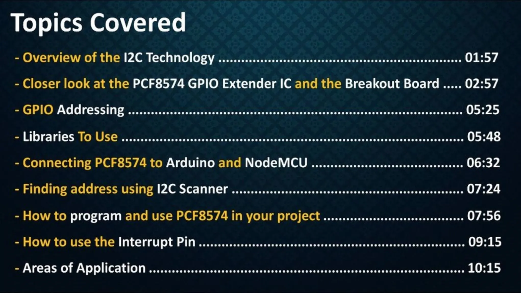
- Overview of the I2C Technology
- Closer look at the PCF8574 GPIO Extender IC and the Breakout Board
- GPIO Addressing
- Libraries To Use
- Connecting PCF8574 to Arduino and NodeMCU
- Finding address using I2C Scanner
- How to program and use PCF8574 in your project
- How to use the Interrupt Pin
- Areas of Application
Step 3: I2C Technology
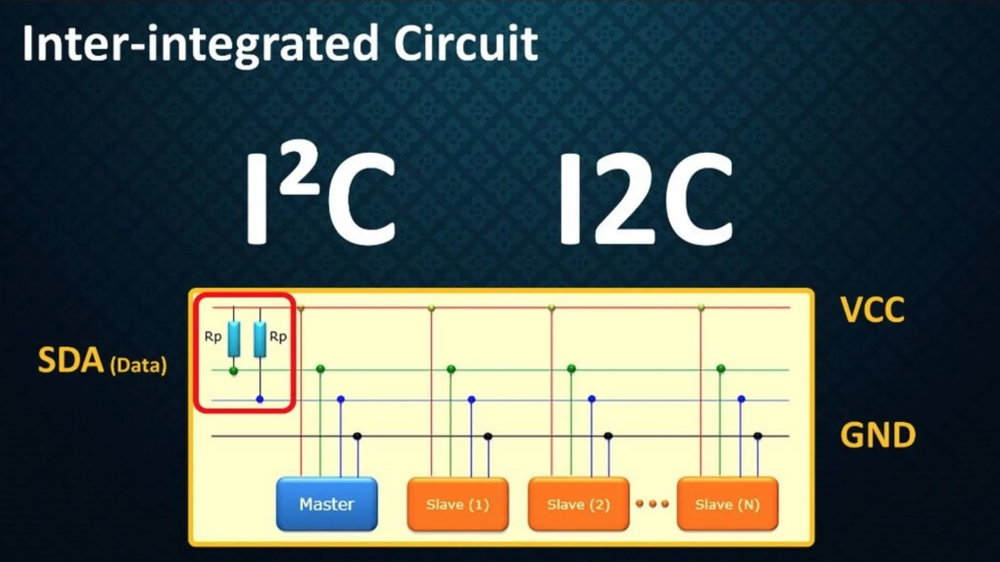
Inter-integrated Circuit pronounced I-squared-C (I²C) or I2C is a 'short distance', 'two-wire bus technology' (well actually 4 wires because you also need the VCC and Ground) that is used for 'serial communication' between multiple processors and sensors.
If you want to know more about the I2C technology please check out my 'Tutorial Number 09'. For now, we will just cover the basics of I2C and we will jump to our main topic. The two wires are:
- SDA - Serial Data (data line) and
- SCL - Serial Clock (clock line)
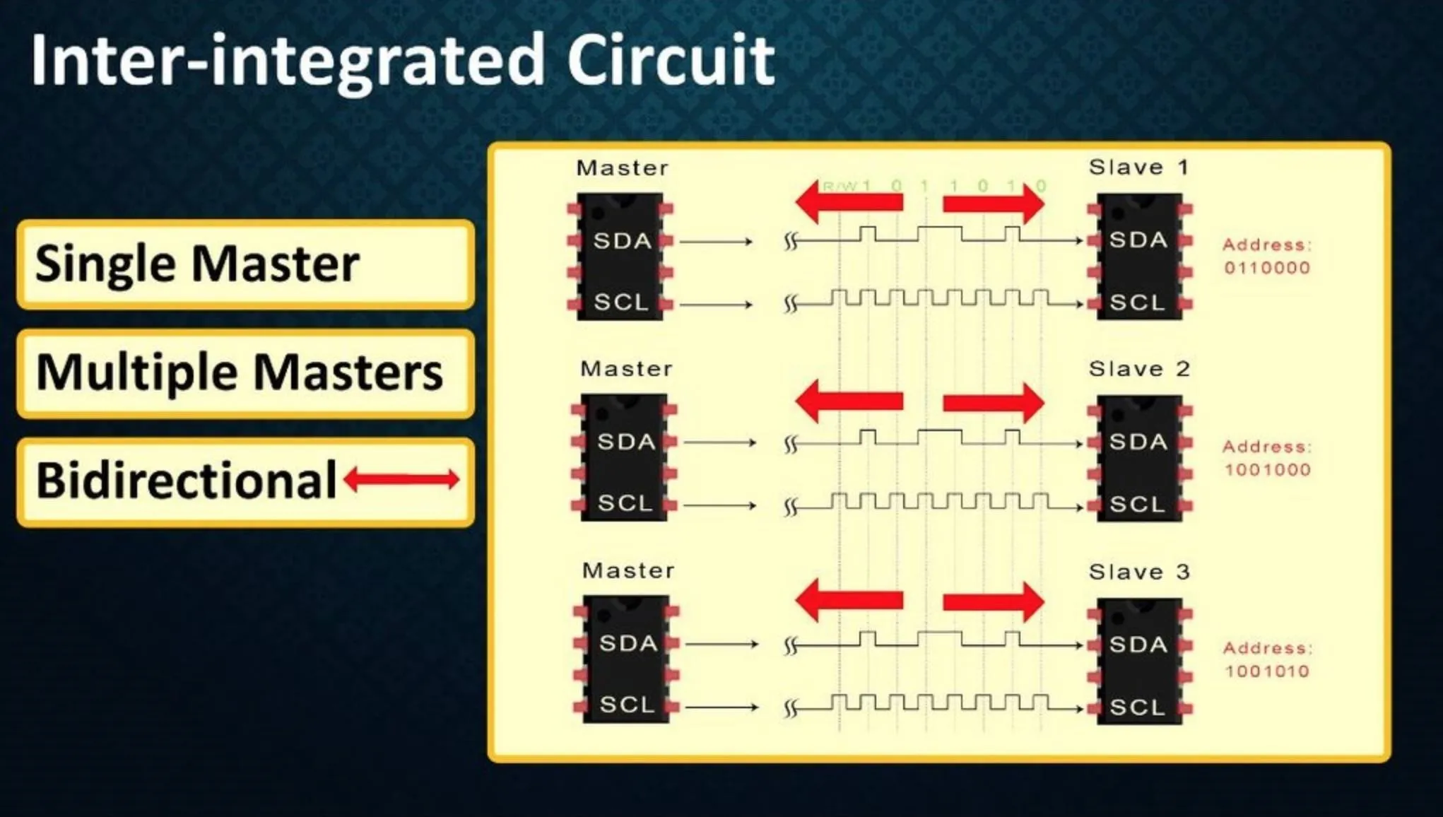
Both of these lines are open-drain and are pulled-up with resistors. Usually, there is one master and one or multiple slaves on the line, however, there can be multiple masters as well. Both masters and slaves can transmit or receive data.
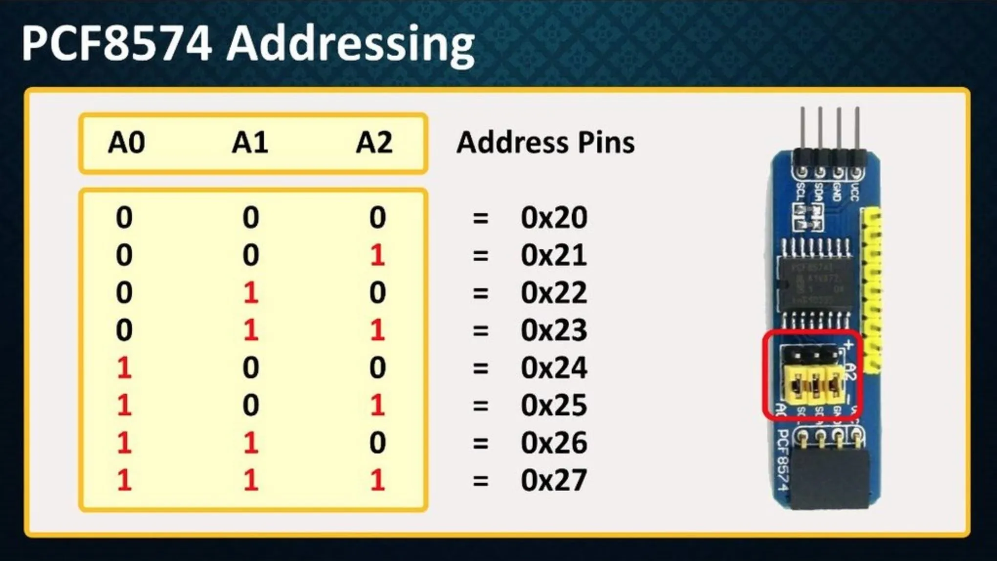
PCF8574 GPIO Extender run on the I2C bus, extending the 'IO Pins' which can be controlled by a single host I2C bus. The Address range of PCF8574 is from 0x20 to 0x27 (7 bit address mode). at the max 8 of these devices can be connected in a project to the I2C bus.


Step 4: Closer Look / Pinouts
IC: (5 pieces for AUD $2.30)
**************
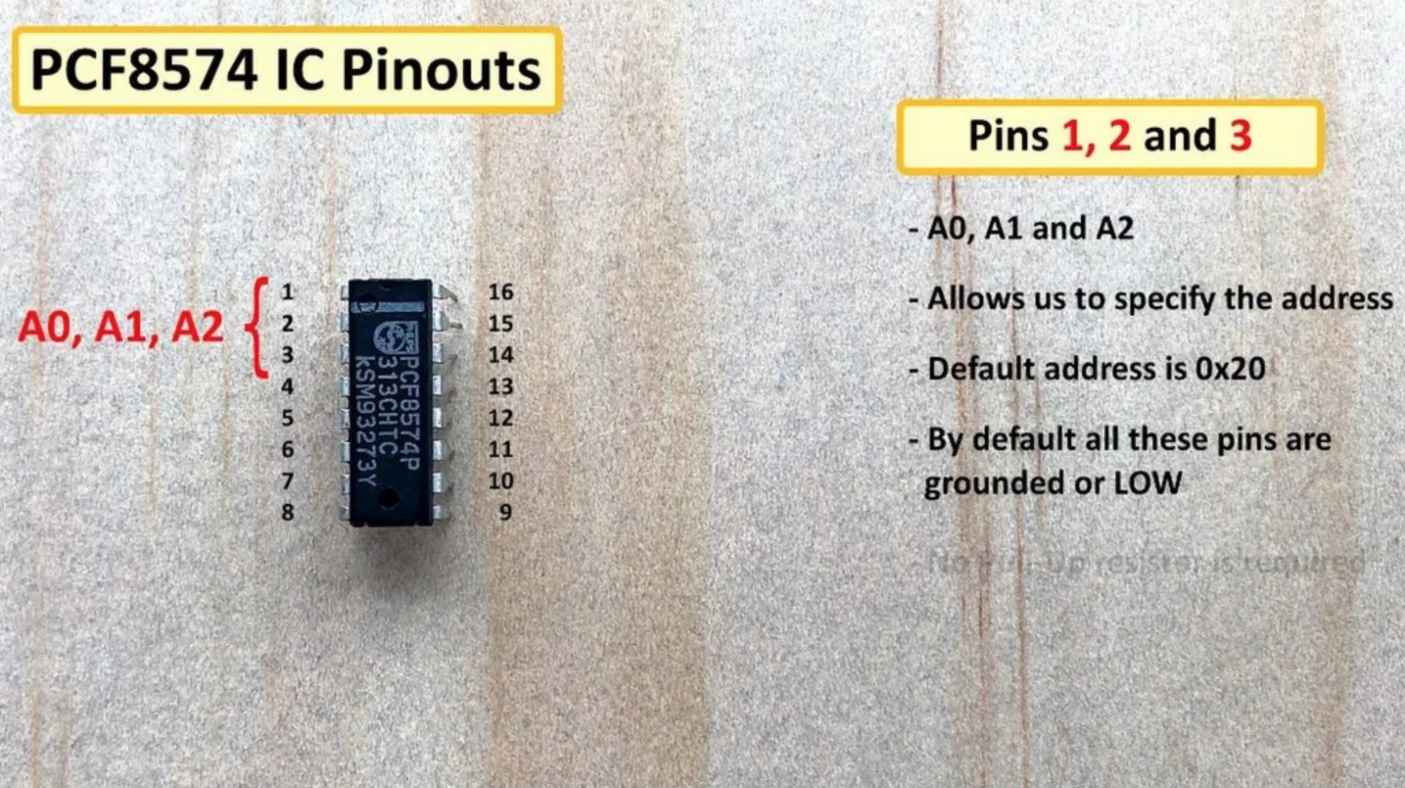
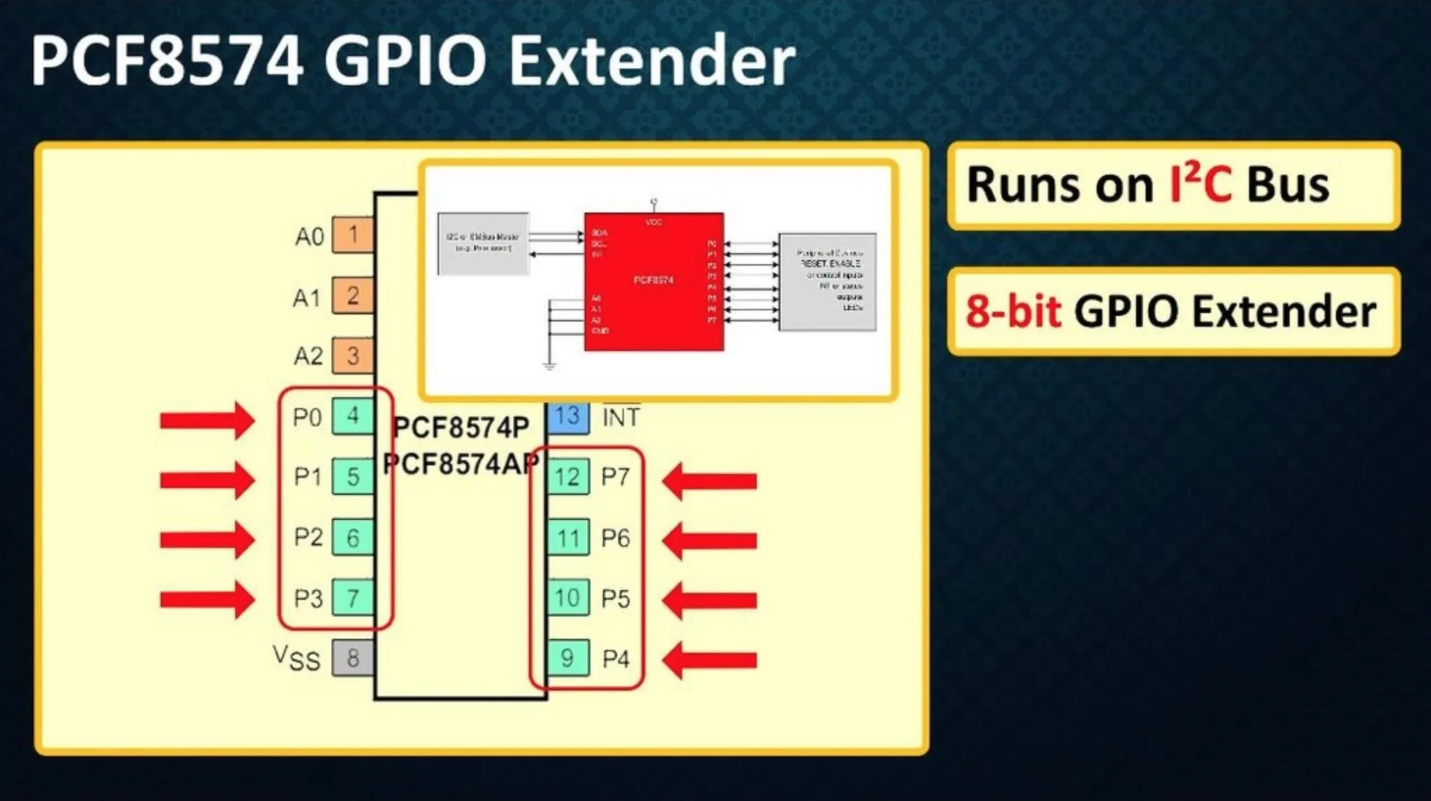
Lets first checkout the pin-outs of the PCF8574 IC:
- Pin 16 of this IC is VCC which can operate on 2.5V to 6V
- Pin 8 is GND
- Pins 4~7 and 9~12 are the P0 to P7 8-Parallel (which means you can use all the 8 pins at once) I/O pins. Each of these bidirectional I/O pins can be used as an input or output without the use of a data-direction control signal. At power on, all these I/O pins are at HIGH state.
- Pin 15 is for the I2C serial data input or output (Connect to VCC through a pull-up resistor) and
- Pin 14 is for the I2C clock input (Connect to VCC through a pull-up resistor)
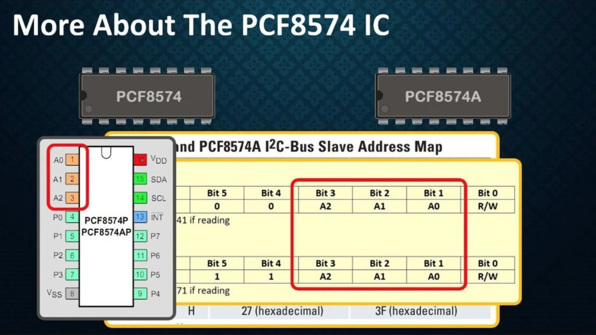
- Pins 1, 2, and 3 or the A0, A1 and A2 allows us to specify the address that the PCF8574 appears as on the I2C bus by turning them HIGH. Default address is 0x20. By default all these pins are grounded or LOW. Pull-up resistors are not needed for these pins.
- Pin 13 is for the Interrupt Output. Connect it to the VCC using a pull-up resistor.
- These ICs have very "Low Standby-Current" Consumption of only 10µA.
- The SDA, SLC and the Interrupt pins all need to be pulled up using pull-up resistors
- There is a second variant of this IC available in the market called the PCF8574A. The major difference is the addressing scheme. The first four bits of the PCF8574's 7-bit address are 0100, and those for the PCF8574A are 0111. The lower three bits are the settings on the device pins A2, A1, and A0.
- The PCF8574 and PCF8574A have a maximum sinking current of 25mA. In applications requiring additional drive, two port pins may be connected together to sink up to 50mA current.


Step 5: Module
(1 Board for AUD $1.34)
****************
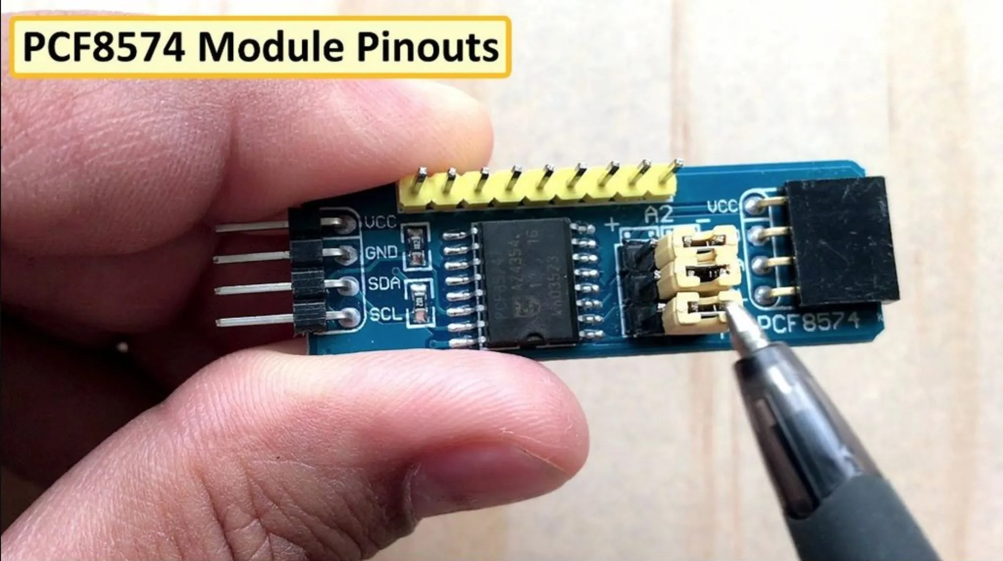
- Now lets have a look at the PCF8574 Break-outboard:
- Looking from left to right we can see that the module has 4 pins: VCC, GND, SDA and SCL
- Then we have the two 10kO SMD pull-up resistors for the SDA and SCL buses.
- Next we have the PCF8574 SMD IC followed by the 3 jumpers for A0, A1 and A2 with high and low positions. Then we have these ports which can be used to piggyback another one of these boards.
- Then we have the 8 I/O pins plus one Interrupt pin. If we look at the back of the board the pins are all labeled starting from P0 to P7 and then ending with the INTrupt pin.
When you are using multiple of these you can switch the address by adjusting these jumperAddress bars.


Step 6: Addressing
By connecting the three address bits A0, A1 and A2 to VIN or HIGH you can get different combination of the addresses.
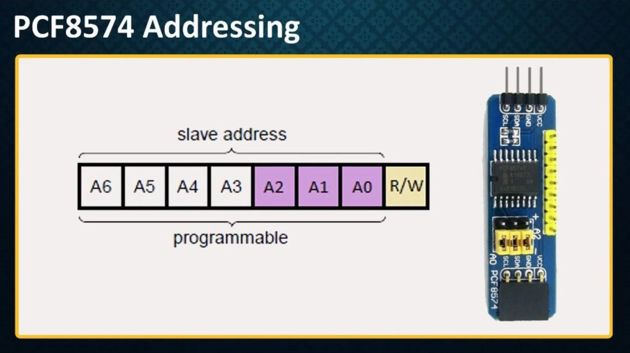
This is how an address byte of the PCF8574 looks like. First 7-bits combine to form the slave address. The last bit of the slave address defines the operation (read or write) to be performed. When it is high (1), a read is selected, while a low (0) selects a write operation.


Step 7: Library to Use
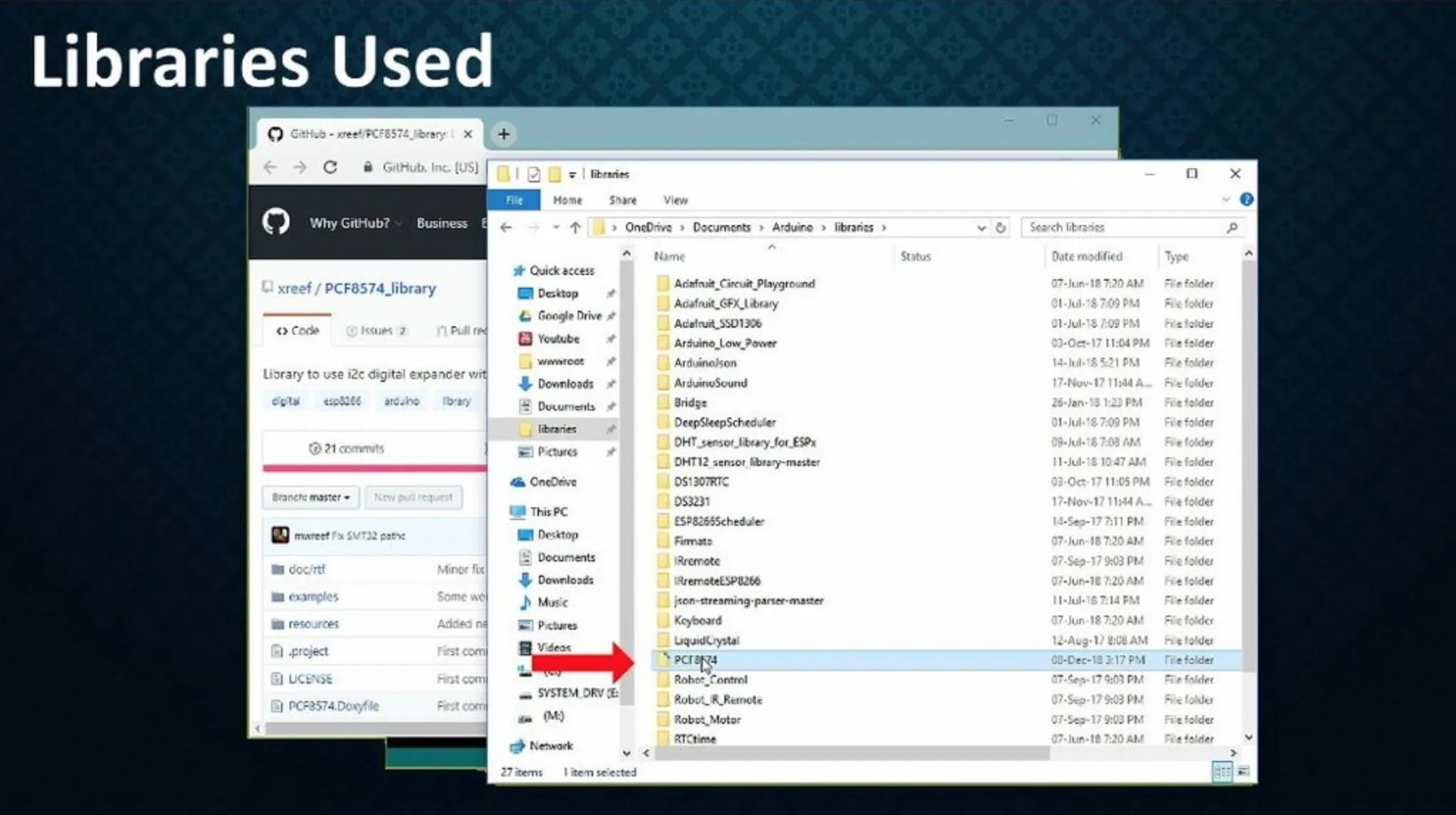
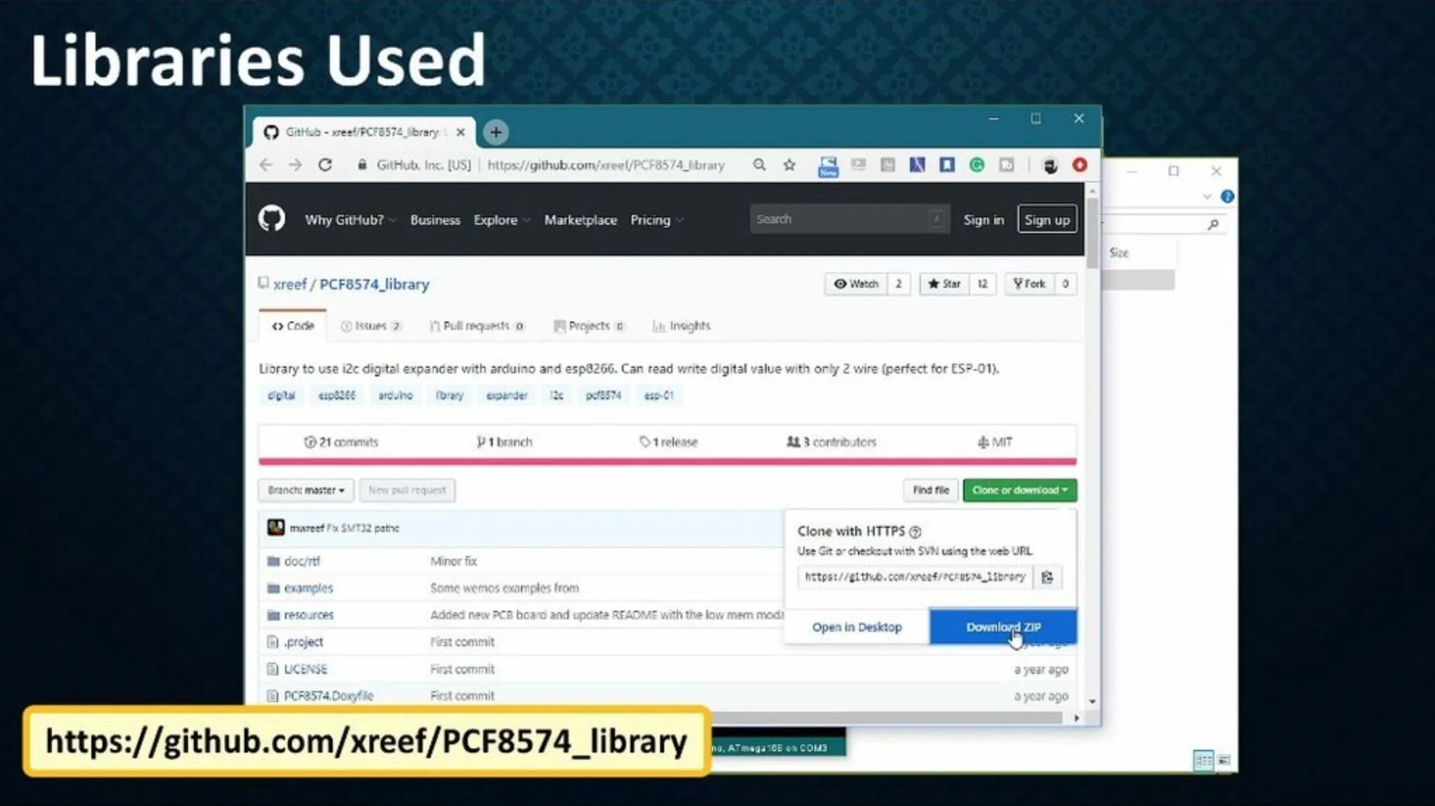
The included 'Wire Library' allows to communication over the I2C/TWI bus of Arduino, however if you want you can also download and use the 'PCF8574_library' from github: github.com/xreef/PCF8574_library
The link is in the description below. Click the DOWNLOADS button in the top right corner of the page, once downloaded rename the uncompressed folder to PCF8574.
Make sure that the PCF8574 folder contains PCF8574.cpp and PCF8574.h.
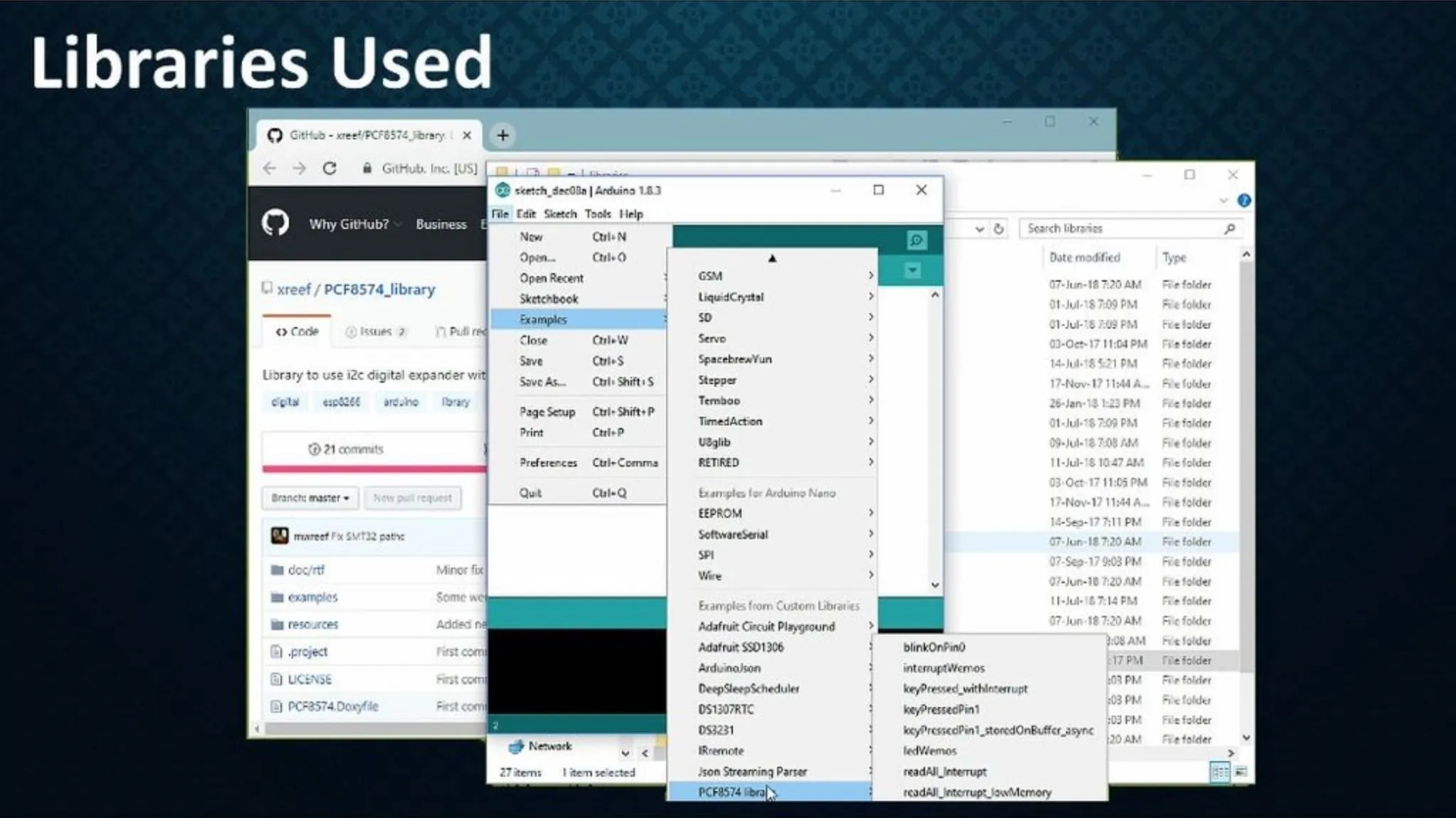
Place the PCF8574 library folder in your Arduino /libraries/ folder.
You may need to create the libraries sub-folder if this is your first library. Restart the IDE and then you should be able to use the library in your code. This library also comes with very good examples which will help you in getting your hands on the IO Expander.
#include "Arduino.h"
#include "PCF8574.h"Attachments


Step 8: How to Connect to Arduino/NodeMCU
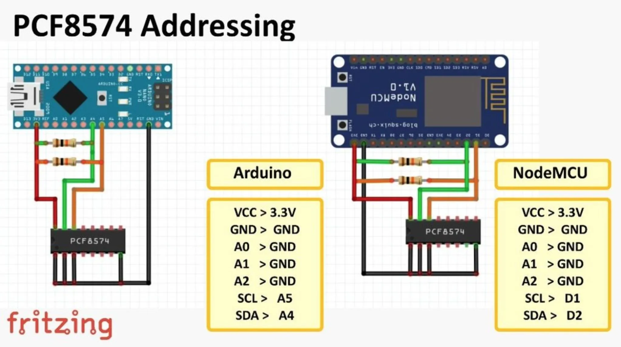
Lets start by connecting the IC to an Arduino. Connect
- VCC to 3.3v
- GND to GND
We also need to connect the three address selection pins A0, A1 and A2 to GND to use the default 0x20 address Then connect the SCL pin to A5 of Arduino and
- SDA to A4
Finally we need to pull-up both the SCL and SDA buses with 10K resistors respectively.
For NodeMCU connect:
- VCC to 3.3v
- GND to GND
- Pins A0, A1 and A2 to GND
- SCL to D1
- SDA to D2
And finally pull-up both the SDA and SCL buses using 10K resistors respectively
Once the IC is hooked up to the micro-controller, you just need to connect the sensors to the Pins 4~7/9~12 or in other words to the pins P0 to P7 of the IC.
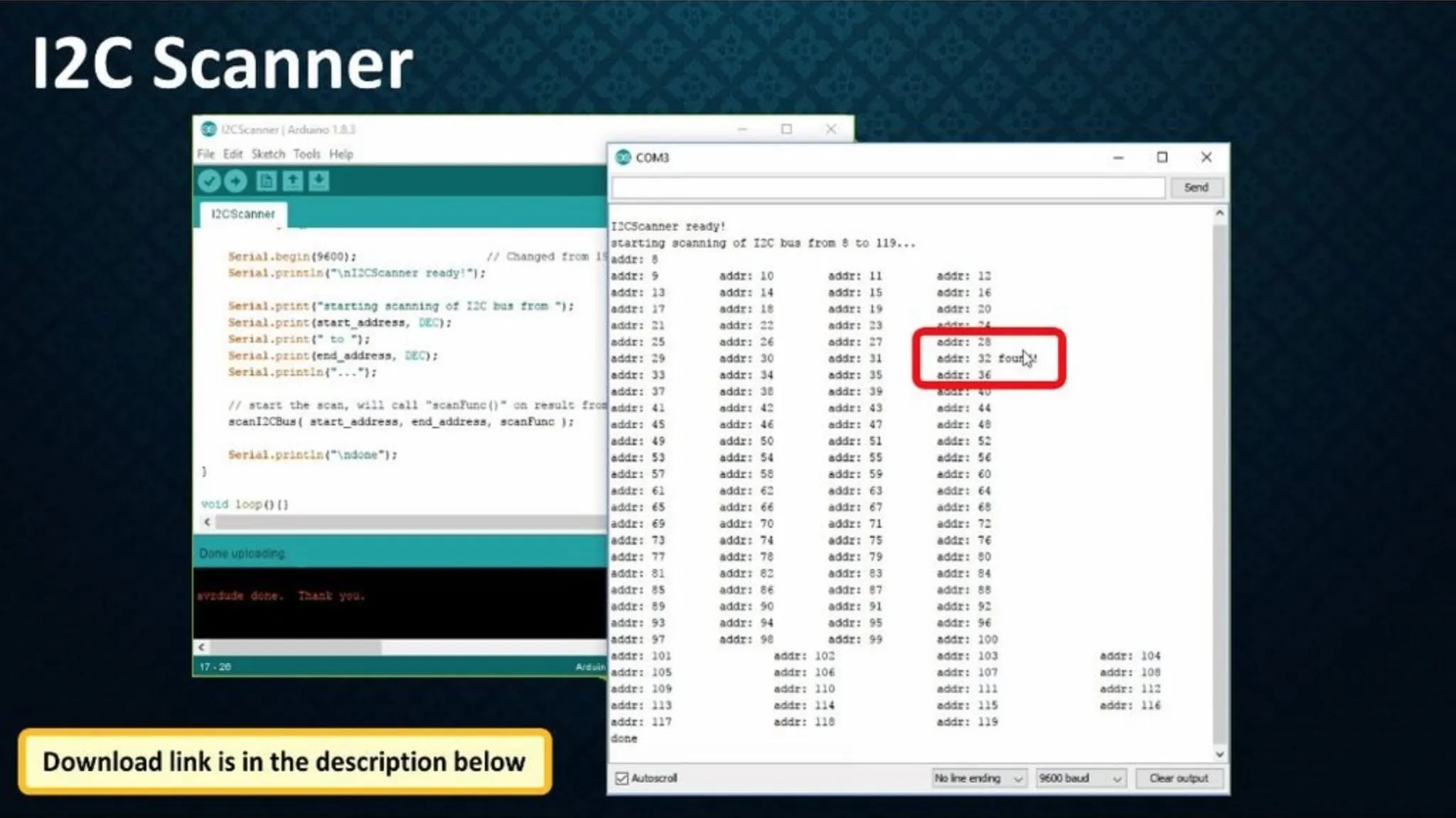
Step 9: I2C Scanner
As we know, by connecting the three address bits A0, A1 and A2 to VIN or HIGH we can get different combination of addresses. Therefore, it sometimes becomes hard to figure out what address has been allocated to the expander. Moreover, if there are two or more devices on the I2C bus it is always a good idea to check if any one of them is conflicting with other one.
By running this 'I2C Scanner' you can easily find the hex address of your device. When loaded to an Arduino, the sketch scans the I2C network, showing the addresses that respond.
Step 10: The Code
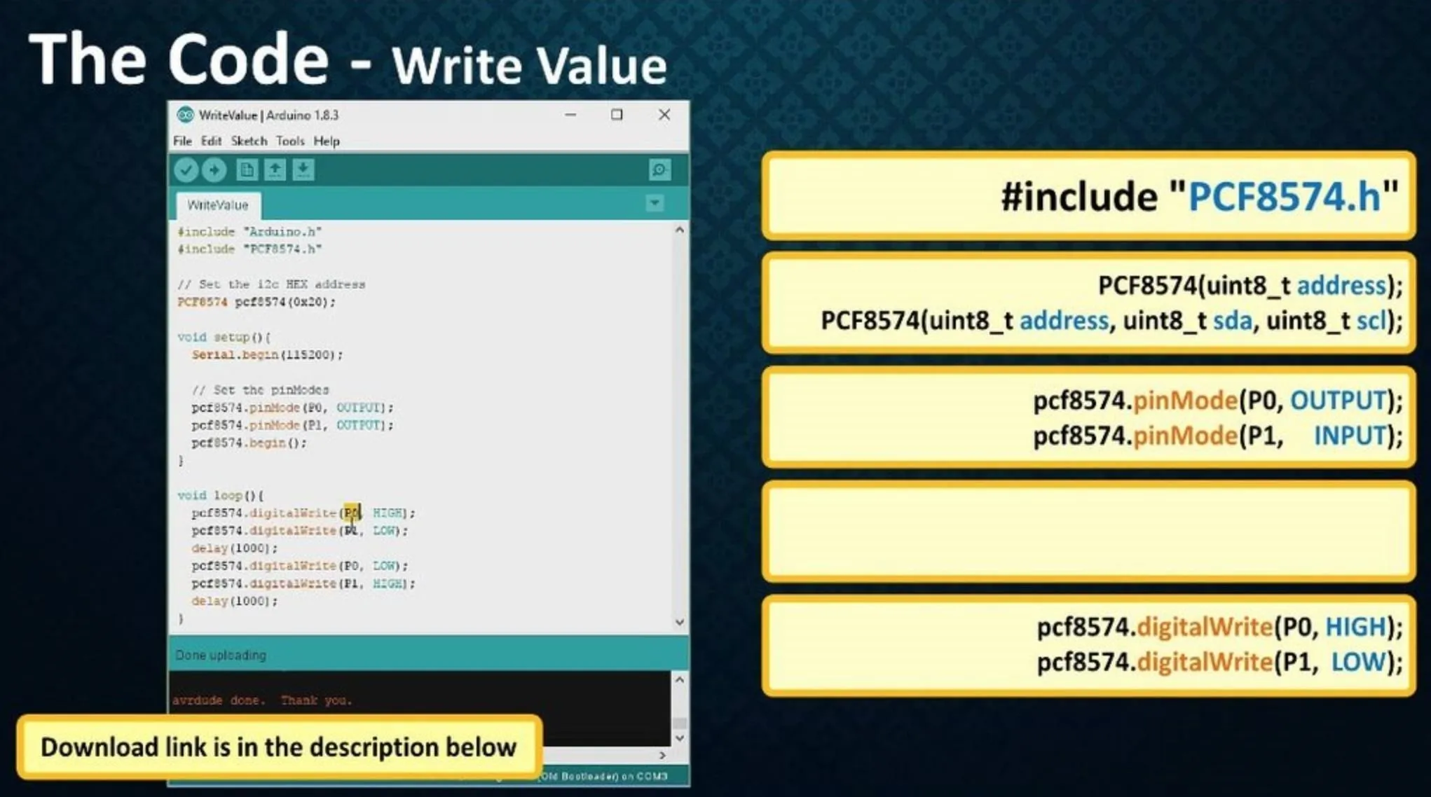
Once you know the address of the IO Expander you can easily use it in your code.
First you need to include the "PCF8574.h" library to your code. Then you need to pass the address of IO Expander to the constructor:
PCF8574(uint8_t address);for esp8266 if you want specify SDA and SCL pin use this:
PCF8574(uint8_t address, uint8_t sda, uint8_t scl);Then you need to specify the modes of the IO pins:
pcf8574.pinMode(P0, OUTPUT);
pcf8574.pinMode(P1, INPUT);
and finally "begin" the transmission before looping through the rest of the code.
Step 11: Write
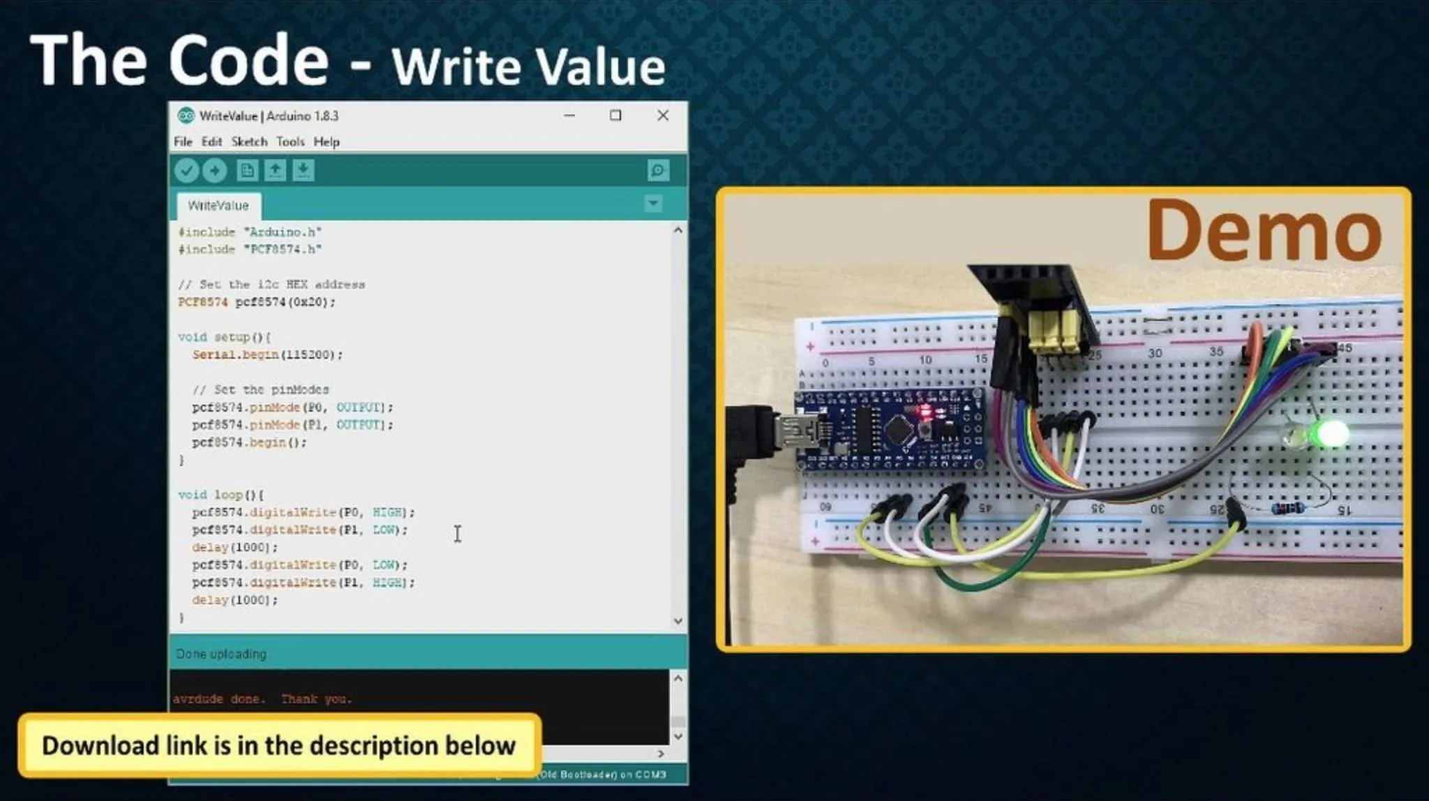
ValueNow, to write a value, you just need to call the "digitalWrite" function and pass the pin-number followed by the mode:
PCF8574.digitalWrite(P1, HIGH);or:
PCF8574.digitalWrite(P1, LOW);Alright, so lets upload the code to an Arduino. As per the code the LEDs attached to P0 and P1 of the expander should alternate and blink, and thats exactly whats happening here, bingo.


Step 12: Read Value
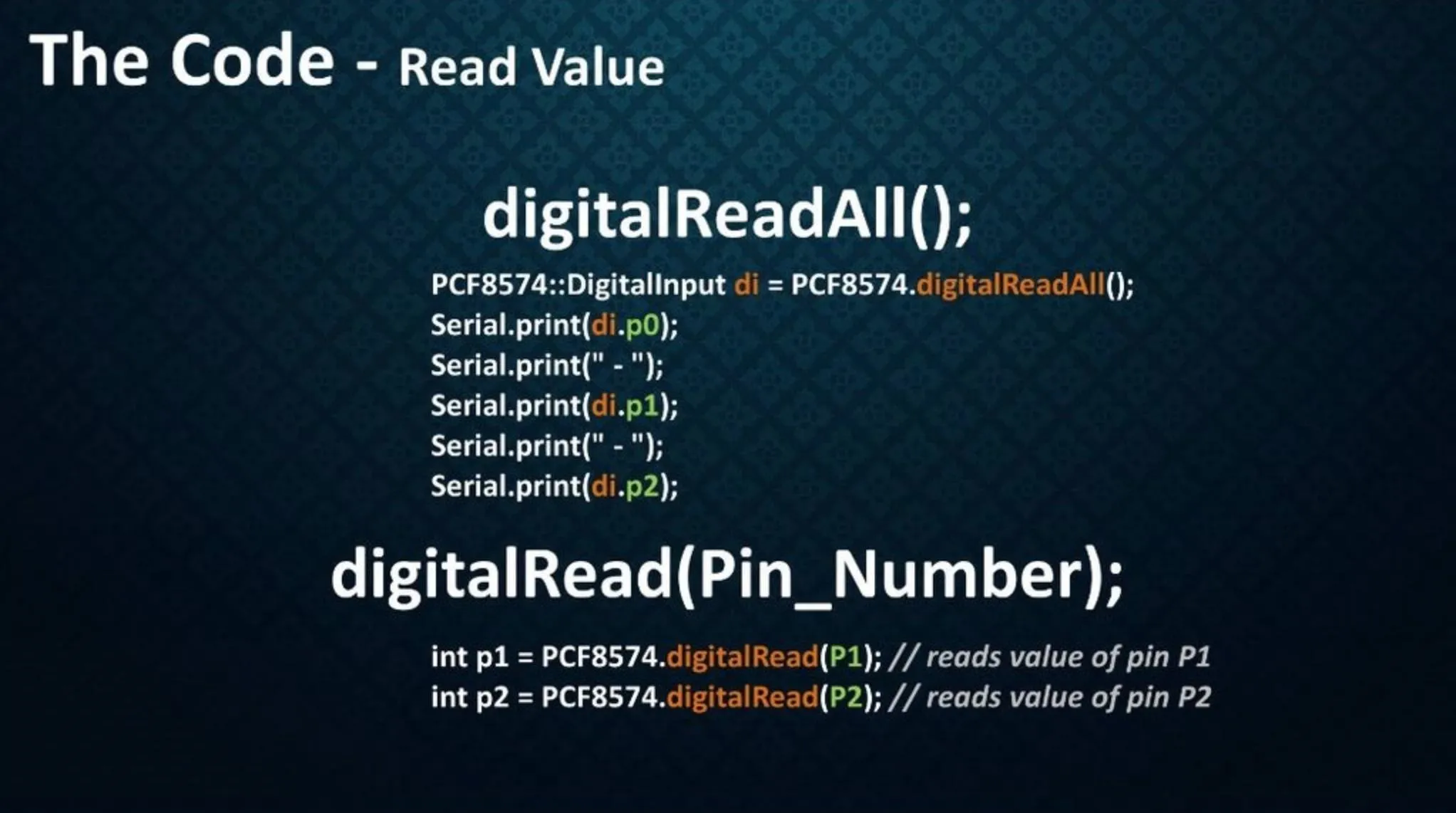
Now, to read values from the expander we are going to use either one of the two functions the "digitalReadAll()" or "digitalRead(Pin_Number)".
digitalReadAll() function reads 'all the input pins' in one transmission:
PCF8574::DigitalInput di = PCF8574.digitalReadAll();
Serial.print(di.p0); Serial.print(" - ");
Serial.print(di.p1); Serial.print(" - ");
Serial.print(di.p2); Serial.print(" - ");
Serial.println(di.p3);
If you want read a single input you can use the "digitalRead(Pin_Number)" function:
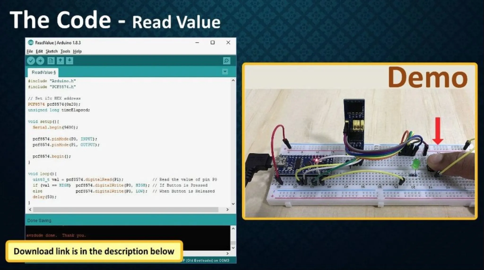
int p1 = PCF8574.digitalRead(P1); // reads pin P1Now, lets load this code to an Arduino. The code is very simple and it just reads the value of the pin P1 in a loop. If the value is HIGH it will turn on the LED connected to the pin P0. I am using this pushbutton to change the state of the pin P1. When the button is pressed, value of P1 goes HIGH and the LED lights up, and when the button is released the LED goes off, thats it simple.


Step 13: Interrupt Pin
In today's complex, embedded, computing and data-communication systems, interrupts are used extensively to service peripheral devices. However, because of the pin-number limitation on packages, most microprocessors have only one or two interrupt lines.
Consequently, several devices usually are connected to the same interrupt line. The drawback to this configuration is that the overhead processing time to identify the device that requested the interrupt service may be too long (in the order of microseconds).
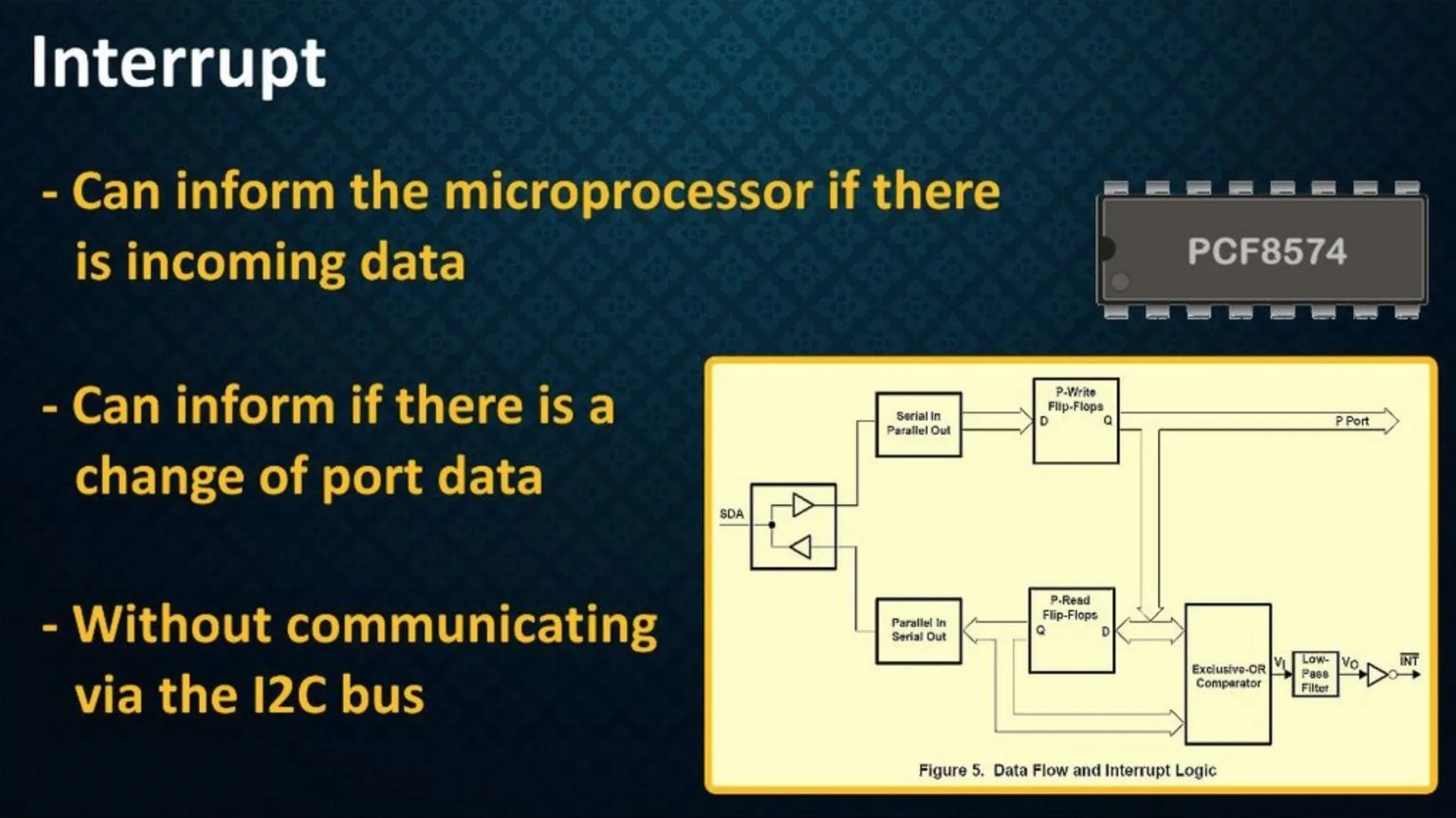
The remote I/O expander can inform the microprocessor if there is incoming data on the port or if there is a change of port data, without having to communicate via the I2C bus.
The PCF8574 provides an open-drain interrupt (INT) output that can be fed to a corresponding input of the microprocessor. To learn more about interrupts, please read the attached datasheet.
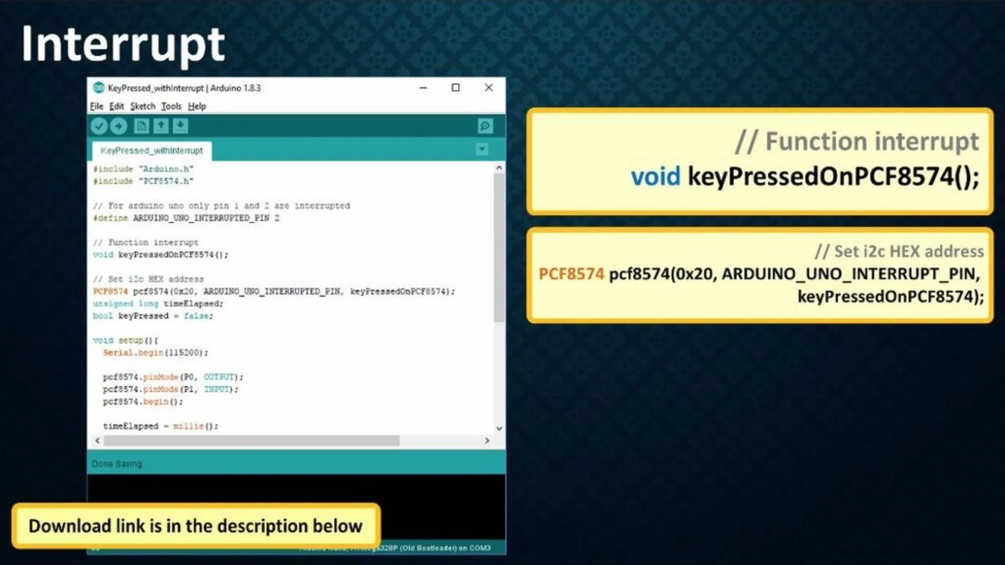
To use interrupts you must initialize the pin and the function to call when PCF8574 raises an interrupt, once done you can use the interrupt routine in your program.
// Function interrupt
void keyPressedOnPCF8574();
// Set i2c HEX address
PCF8574 pcf8574(0x20, ARDUINO_UNO_INTERRUPT_PIN, keyPressedOnPCF8574);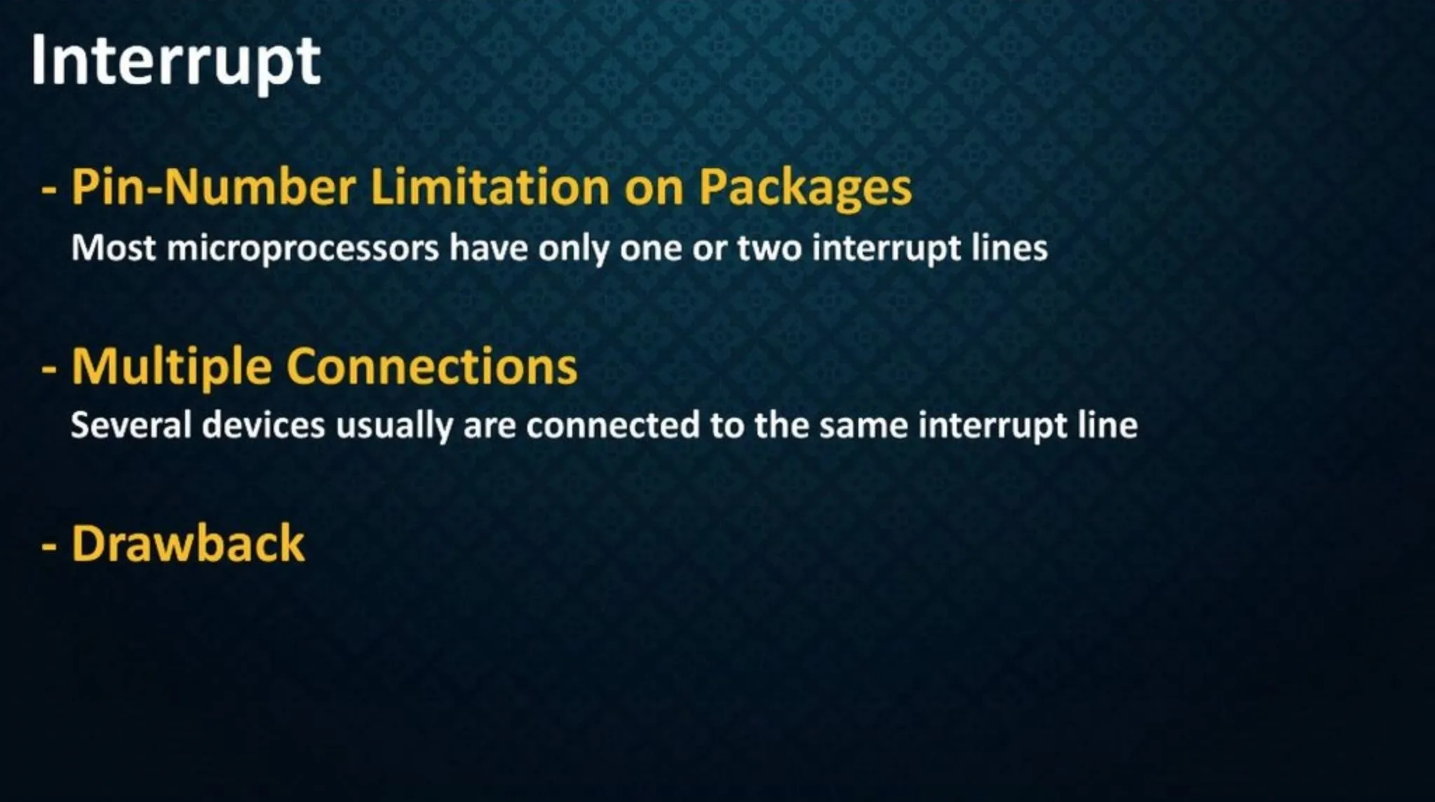


Step 14: Areas of Application
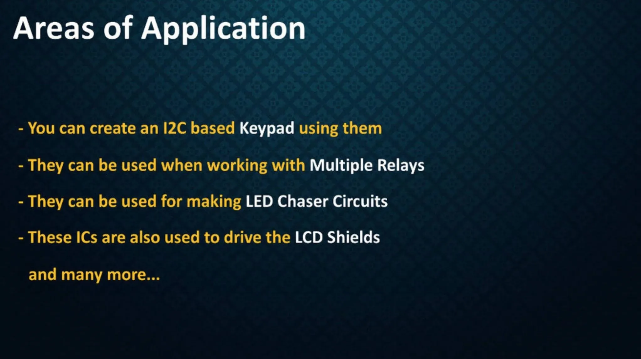
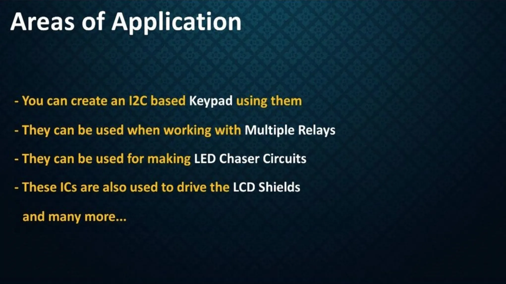
PCF8574 GPIO Extenders are used in:
- Processors with Limited GPIO pins
- You can create an I2C based Keypad using them
- They can be used when working with Multiple Relays
- They can be used for making LED Chaser Circuits
- These ICs are also used to drive the LCD Shields and many more...
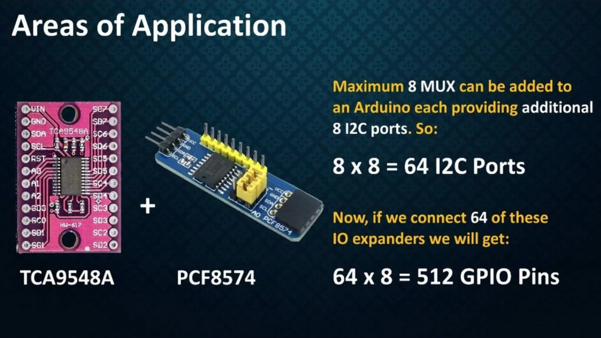
I am actually designing a breakout board with 8 of these ICs pre-fitted on it to extend my Arduino's GPIO pins. In another attempt, I am going to couple these ICs with the TCA9548A I2C MUX to see if I can get 512 GPIO pins in total. The TCA9548A Breakout enables communication with multiple I2C devices that have the same address making it simple to interface with them. Obviously, NANO will cry controlling that many pins but may be MEGA will be able to handle it. However, I haven't actually tried it yet.
Maximum 8 MUX can be added to an Arduino each providing additional 8 I2C ports. So:
8 x 8 = 64 I2C Ports
Now, if we connect 64 of these IO expanders we will get:
64 x 8 = 512 IO Pins
So, what are you waiting for? Go ahead use your imagination and attach 64 sensors to your Arduino to make an amazing automation project to amaze your friends.


That's It
You can also see this tutorial on my Instructable. Thanks again for reading the tutorial. I hope it helps you. If you want to support me you can subscribe to my channel and watch my other videos. Thanks again, bye now.


Comments
No Comments Exist
Be the first, drop a comment!